- 您现在的位置:买卖IC网 > Sheet目录3882 > PIC18F1320T-E/ML (Microchip Technology)IC MCU FLASH 4KX16 EEPROM 28QFN
PIC18F1220/1320
DS39605F-page 6
2007 Microchip Technology Inc.
1.3
Details on Individual Family
Members
Devices in the PIC18F1220/1320 family are available
in 18-pin, 20-pin and 28-pin packages. A block diagram
for this device family is shown in Figure 1-1.
The devices are differentiated from each other only in
the amount of on-chip Flash program memory
(4 Kbytes for the PIC18F1220 device, 8 Kbytes for the
PIC18F1320 device). These and other features are
summarized in Table 1-1.
A block diagram of the PIC18F1220/1320 device
architecture is provided in Figure 1-1. The pinouts for
this device family are listed in Table 1-2.
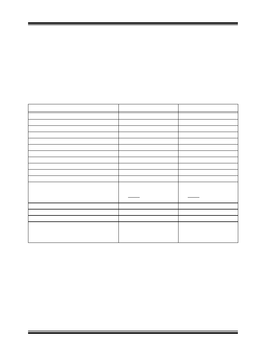
TABLE 1-1:
DEVICE FEATURES
Features
PIC18F1220
PIC18F1320
Operating Frequency
DC – 40 MHz
Program Memory (Bytes)
4096
8192
Program Memory (Instructions)
2048
4096
Data Memory (Bytes)
256
Data EEPROM Memory (Bytes)
256
Interrupt Sources
15
I/O Ports
Ports A, B
Timers
4
Enhanced Capture/Compare/PWM Modules
1
Serial Communications
Enhanced USART
10-bit Analog-to-Digital Module
7 input channels
Resets (and Delays)
POR, BOR,
RESET
Instruction, Stack Full,
Stack Underflow (PWRT, OST),
MCLR (optional), WDT
POR, BOR,
RESET
Instruction, Stack Full,
Stack Underflow (PWRT, OST),
MCLR (optional), WDT
Programmable Low-Voltage Detect
Yes
Programmable Brown-out Reset
Yes
Instruction Set
75 Instructions
Packages
18-pin SDIP
18-pin SOIC
20-pin SSOP
28-pin QFN
18-pin SDIP
18-pin SOIC
20-pin SSOP
28-pin QFN
发布紧急采购,3分钟左右您将得到回复。
相关PDF资料
PIC16LF87T-I/ML
IC MCU FLASH 4KX14 EEPROM 28QFN
PIC18F25J10-I/SS
IC PIC MCU FLASH 16KX16 28SSOP
PIC16F88T-E/SS
IC MCU FLASH 4KX14 EEPROM 20SSOP
PIC16C621A-04/SO
IC MCU OTP 1KX14 COMP 18SOIC
PIC16F88T-E/ML
IC MCU FLASH 4KX14 EEPROM 28QFN
PIC16F88T-E/SO
IC MCU FLASH 4KX14 EEPROM 18SOIC
PIC16F882-I/SO
IC PIC MCU FLASH 2KX14 28SOIC
PIC16F87T-E/SS
IC MCU FLASH 4KX14 EEPROM 20SSOP
相关代理商/技术参数
PIC18F1320T-E/SO
制造商:Microchip Technology Inc 功能描述:PIC18 Series 256 B RAM 8 kB Flash 8-Bit Enhanced Microcontroller - SOIC-18
PIC18F1320T-I/ML
功能描述:8位微控制器 -MCU 8KB 256 RAM 16 I/O RoHS:否 制造商:Silicon Labs 核心:8051 处理器系列:C8051F39x 数据总线宽度:8 bit 最大时钟频率:50 MHz 程序存储器大小:16 KB 数据 RAM 大小:1 KB 片上 ADC:Yes 工作电源电压:1.8 V to 3.6 V 工作温度范围:- 40 C to + 105 C 封装 / 箱体:QFN-20 安装风格:SMD/SMT
PIC18F1320T-I/SO
功能描述:8位微控制器 -MCU 8KB 256 RAM 16 I/O RoHS:否 制造商:Silicon Labs 核心:8051 处理器系列:C8051F39x 数据总线宽度:8 bit 最大时钟频率:50 MHz 程序存储器大小:16 KB 数据 RAM 大小:1 KB 片上 ADC:Yes 工作电源电压:1.8 V to 3.6 V 工作温度范围:- 40 C to + 105 C 封装 / 箱体:QFN-20 安装风格:SMD/SMT
PIC18F1320T-I/SOG
功能描述:8位微控制器 -MCU 8KB 256 RAM 16 I/O Lead Free Package RoHS:否 制造商:Silicon Labs 核心:8051 处理器系列:C8051F39x 数据总线宽度:8 bit 最大时钟频率:50 MHz 程序存储器大小:16 KB 数据 RAM 大小:1 KB 片上 ADC:Yes 工作电源电压:1.8 V to 3.6 V 工作温度范围:- 40 C to + 105 C 封装 / 箱体:QFN-20 安装风格:SMD/SMT
PIC18F1320T-I/SS
功能描述:8位微控制器 -MCU 8KB 256 RAM 16 I/O RoHS:否 制造商:Silicon Labs 核心:8051 处理器系列:C8051F39x 数据总线宽度:8 bit 最大时钟频率:50 MHz 程序存储器大小:16 KB 数据 RAM 大小:1 KB 片上 ADC:Yes 工作电源电压:1.8 V to 3.6 V 工作温度范围:- 40 C to + 105 C 封装 / 箱体:QFN-20 安装风格:SMD/SMT
PIC18F1330-E/ML
功能描述:8位微控制器 -MCU 8KB Flash 256 RAM RoHS:否 制造商:Silicon Labs 核心:8051 处理器系列:C8051F39x 数据总线宽度:8 bit 最大时钟频率:50 MHz 程序存储器大小:16 KB 数据 RAM 大小:1 KB 片上 ADC:Yes 工作电源电压:1.8 V to 3.6 V 工作温度范围:- 40 C to + 105 C 封装 / 箱体:QFN-20 安装风格:SMD/SMT
PIC18F1330-E/P
功能描述:8位微控制器 -MCU 8KB Flash 256 RAM RoHS:否 制造商:Silicon Labs 核心:8051 处理器系列:C8051F39x 数据总线宽度:8 bit 最大时钟频率:50 MHz 程序存储器大小:16 KB 数据 RAM 大小:1 KB 片上 ADC:Yes 工作电源电压:1.8 V to 3.6 V 工作温度范围:- 40 C to + 105 C 封装 / 箱体:QFN-20 安装风格:SMD/SMT
PIC18F1330-E/SO
功能描述:8位微控制器 -MCU 8KB Flash 256 RAM RoHS:否 制造商:Silicon Labs 核心:8051 处理器系列:C8051F39x 数据总线宽度:8 bit 最大时钟频率:50 MHz 程序存储器大小:16 KB 数据 RAM 大小:1 KB 片上 ADC:Yes 工作电源电压:1.8 V to 3.6 V 工作温度范围:- 40 C to + 105 C 封装 / 箱体:QFN-20 安装风格:SMD/SMT